Welcome to the second part of the Colorlight 5A-75B article. You can find the first part here.
In this blogpost I will show you how to set up, synthesize and program your first Verilog program on the ECP5 FPGA using the Yosys suite.
# The FPGA toolchain
The FPGA workflow consists of a few more steps compared to the usual software toolchain workflow.
The Verilog source, which is a description of the logic that makes up the FPGA design, first needs to be synthesized.
The synthesis process scans through all the source files and libraries to find out the hierarchy of the modules, starting with the specified top module.
The result of this process is a low level logical representation of all the abstract components that will make up the final design.
In the FPGA flow, this step is done by the yosys program, and results in a JSON file.
The next step in the toolchain is place-and-route.
This is where the process becomes specific to the target FPGA family, because it takes the abstract components and maps it to physical parts that make up the FPGA.
The logical design is translated into configuration data for all the switches, lookup tables and registers in the FPGA’s macroblocks.
Yosys suite includes the Nextpnr tool which does this step.
For our board, which runs on the Lattice ECP5 fpga, we will have to use the nextpnr-ecp5 program.
This will give us a .config file which represents the configuration of the fpga.
The last step is to upload the configuration data to the target FPGA.
This step can have many forms, but in Yosys it has two parts: packing and uploading.
First, the configuration data needs to be packed into a format that is recognized by the FPGA controller.
This is done with the ecppack executable. We will use ecppack to create an SVF (Serial Vector Format).
The SVF is a pretty ingenious hack - the file contains plain JTAG commands that need to be sent to the target, which makes it independent from the JTAG adapter.
Using SVF, in principle, you can program any JTAG device with any JTAG adapter.
The second part is the actual upload of the SVF to the device.
We will use openocd to communicate with our JTAG adapter and upload the SVF file with configuration data to it. After the upload is complete, the FPGA will start running.
# Hello, blink!
For our journey into getting the board to blink, we will use the following Verilog. It’s a simple clock divisor module whose output is connected to an IO pin on the FPGA that is connected to the onboard LED.
module top(input clk_i, output led_o);
   reg  led_reg;
   wire baseclk;

   clkdiv #(.DIV(2000000)) slowclk (clk_i, baseclk);

   always @(posedge baseclk) begin;
      led_reg <= !led_reg;
   end

   assign led_o = led_reg;
endmodule


module clkdiv #(parameter DIV = 24'd5000)(
    input wire clk_i,
    output wire clk_o
    );

    reg [24:0] count = 25'b0;
    reg clk_o_internal = 1;
    //on this board we have a 25MHz clock

    always @(posedge clk_i) begin
        count <= count + 25'b1;
        if(count == DIV) begin
            count <= 25'b0;
            clk_o_internal <= ~clk_o_internal;
        end
    end
    assign clk_o = clk_o_internal;
endmodule
This piece of Verilog will take the clock input from the onboard oscillator, divide it by 500 thousand and output the divided clock to output led_o.
I’ve called the file blink.v. Now we need to synthesize it using yosys:
yosys -p "synth_ecp5 -top top -json blink.json" blink.v
It is important to specify the top module by name using the -top <name> option.
Otherwise yosys may pick the wrong module as the top and later cause an error due to unconstrained IOs.
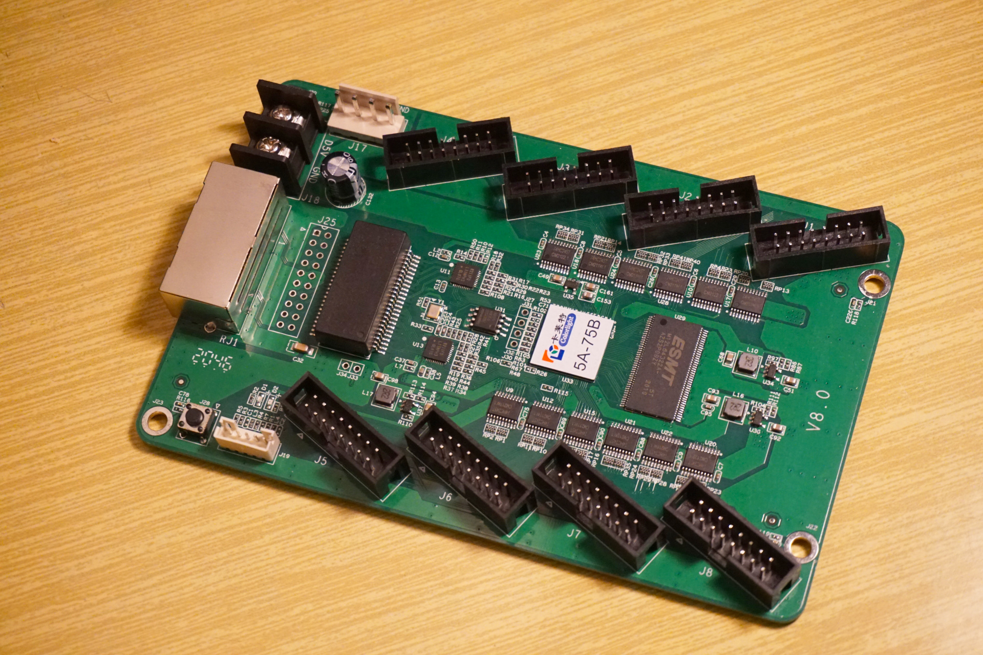
The next step is to assign the logic IOs from the verilog modules to physical pins on the FPGA. This is necesary for the Place and Route step and is done by a constraints file. Looking up q3k’s repository on the 5A-75B board we can find out that the clock is connected to FPGA pin P6, and the onboard led is connected to T6. Here is how the LPF file looks like. I saved it as blink.lpf:
LOCATE COMP "clk_i" SITE "P6";
IOBUF PORT "clk_i" IO_TYPE=LVCMOS33;

LOCATE COMP "led_o" SITE "T6";
IOBUF PORT "led_o" IO_TYPE=LVCMOS25;
Now we can run the Place and Route program, nextpnr-ecp5:
nextpnr-ecp5 --json blink.json --textcfg blink_out.config --25k --package CABGA256 --lpf blink.lpf
We specify the parameters of the ECP5 FPGA: device type LFE5U-25F (--25k) and the package type.
With the output config file all we need to do is to pack the bitstream into an SVF file:
ecppack --svf blink.svf blink_out.config blink.bit
With the SVF file it’s time to program the bitstream into the FPGA. Connect it to your JTAG adapter and power.
openocd -f colorlight_5a75b.cfg -c "svf -quiet -progress blink.svf; exit"
The file colorlight_5a75b.cfg contains my openocd configuration:
source [find interface/jlink.cfg]
adapter_khz 500
transport select jtag

jtag newtap ecp5 tap -irlen 8 -expected-id 0x41111043

init
scan_chain
targets

svf -tap ecp5.tap -quiet -progress blink.svf
exit
the jtag newtap ... line defines a new Test Access Port that corresponds to the FPGA’s TAP. The first line configures openocd to use a JLink as the adapter. If you have a different adapter, then modify this file to your needs.
The example project, along with a Makefile is available on GitHub
# About the author
Chris “polprog” Lasocki (@polprogpl) is a long time electronics hacker and an aspiring physicist. FPGAs are one of his hobbies and he is currently writing a thesis in that field. His other interests include laser physics as well as embedded programming projects. He runs a blog at polprog.net.