# FazyRV
Welcome to another community spotlight article where we shine a light on open source EDA-related projects. If you want to submit a project, please do so here.
FazyRV is a minimal-area RISC-V core that scales with your needs. It allows you to adapt the data path width to process smaller 1, 2, 4, or 8-bit chunks of the 32-bit operands each clock cycle. In addition, each data path width can be combined with FazyRV’s manifold variants to trade area with performance and find the best-fitting configuration for your system requirements and used technology. FazyRV avoids hand optimizations at the gate level to increase readability and ease modifications, such as adding custom instruction extensions.
# Meinhard Kissich’s Bio

I am a Ph.D. student at Graz University of Technology in Austria. After completing my Master’s degree in Information and Computer Engineering in 2022, I joined the Embedded Architectures & Systems (EAS) Group as a university assistant. My main interests and research areas are RISC-V architectures, FPGA CAD tools, and applied formal verification. I enjoy realizing unique ideas outside convention and evaluating these implementations. For me, it is not just about gathering knowledge but also about sharing it and contributing back to the community. I lead the Real-Time Operating Systems Laboratory course and am always up for discussions and exciting projects.
# What motivated you to make FazyRV?
The fascination of getting the most out of a constrained environment and using even small FPGAs for “big” projects – it is like the digital design equivalent of Can it run Doom?. I became captivated by SERV and how small a system-on-chip design can be. However, there was a gap between the 1-bit bit-serial SERV and prevalent 32-bit cores.
That brings me to a second point: I wanted to explore how a sub-32-bit core scales between a 1-bit bit-serial and a 32-bit core in terms of area and performance. This is where FazyRV started as a scalable RISC-V core.
# What makes you excited about FazyRV?
FazyRV allows scaling the core to the project’s needs in a way that was not available to me before. The fine-grained options can be used to explore the design space and find the best area vs. performance trade-off for the system requirements and target technology. Assume the target technology does not have dual-read-port BRAM primitives available without some area overhead. In this case, you can choose an implementation that serially reads the operands at the expense of one additional clock cycle per instruction. Then, you can synthesize the data path to a width that fits your timing requirements. If it is on edge, you may also experiment with a variant that uses a bypass multiplexer and can save one clock cycle on operand loads. All that is done by just playing around with Verilog parameters.
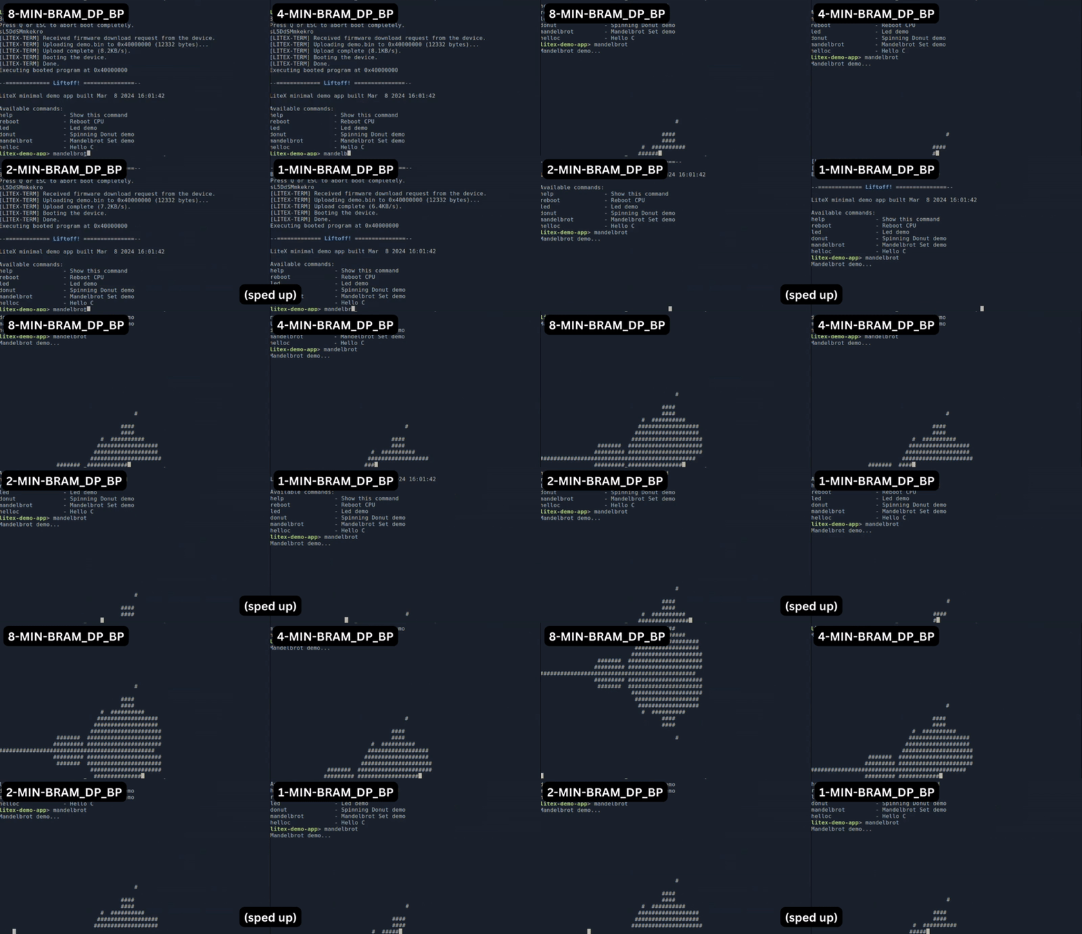
Let us delve into a practical implementation by plotting the Mandelbrot set. The comparison below illustrates the performance disparity when using different chunk sizes. While the variant with an 8-bit chunk size delivers the highest performance, it also results in the largest design, as depicted in the plot at the top.

But there is more to it: FazyRV avoids hand optimization at the gate level. I want to inspect more closely how synthesis tools optimize the current hardware description and map the patterns.
# What are some of the challenges you face?
One was undoubtedly the architecture of shift instructions. The considered designs significantly influence the resulting area and performance. Finding a suitable trade-off is more challenging when the area and performance overhead must fit all data path widths without getting out of balance.
Also, when designing a core highly optimized for area, there are some sacrifices to be made here and there. Of course, the area must be minimized, but likewise, the core must remain suitable for most users and applications when defining constraints in the feature set. One example is the decoder: Not all instruction bits are explicitly checked to reduce the area. Assumptions are made that some instructions cannot occur. The drawback, however, is that an illegal instruction may be interpreted as a different legal instruction instead of raising an illegal instruction exception. In this particular case, it was handled by providing the decoder logic in a table-like format that can be adapted by the user and synthesized to Verilog code by a tool. It eases modifications to detect illegal instructions when required or to add custom instructions to the core without digging into the decoder at a low level. However, many more decisions in the INT and CSR variants are yet to be made.
# What could the community do to support you?
Consider having a play with FazyRV in your next project, either by using the Verilog design directly or exploring FazyRV via LiteX. We are grateful for any opinions, reported issues, or suggestions.
If you want to get involved even more, we maintain a list of open topics in the repository. Feel free to use this as a starting point or bring in your own ideas for discussion or a concrete proposed implementation. Even if you are not involved in digital design, well-designed tooling, workflows, and software support are needed to make adopting FazyRV as convenient as possible and verify changes continuously.
# What is the best link for the project?
The GitHub repository is the best place to start. It is where everything comes together and you will find the latest changes and updates. For example, we will soon publish a research paper with many more evaluations and design insights, which we will reference in the repo.
# What is the best way for people to contact you?
You can find a list of up-to-date contact options on my website.
